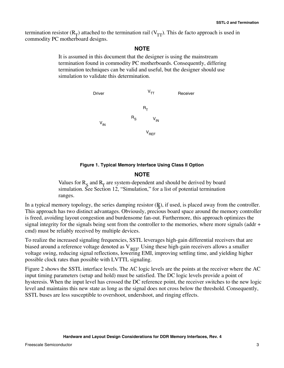
Freescale SemiconductorApplication Note© Freescale Semiconductor, Inc., 2005. All rights reserved. Embedded systems that utilize double data rate memory (DDR) can realize increased performance over traditional single data rate (SDR) memories. As the name implies, DDR enables two data transactions to occur within a single clock cycle without having to double the applied clock or without having to double the size of the data bus. This increased data bus performance is achieved by the introduction of source-synchronous data strobes that permit data to be captured on both the falling and rising edges of the strobe.Although DDR can bring improved performance to an embedded design, care must be observed in the schematic and layout phases to ensure that desired performance is realized. Smaller setup and hold times, cleaner reference voltages, tighter trace matching, new I/O (SSTL-2) signaling, and the need for proper termination can present the board designer with a new set of challenges that were not present for SDR designs. Document Number: AN2582Rev. 4, 10/2005Contents1. SSTL-2 and Termination . . . . . . . . . . . . . . . . . . . . . . 22. DDR Signal Groupings . . . . . . . . . . . . . . . . . . . . . . . . 43. Controller Signal Pin-Out . . . . . . . . . . . . . . . . . . . . . . 54. General Comments About Board Stack-Up . . . . . . . . 65. Layout Order for the DDR Signal Groups . . . . . . . . . 66. Length Matching Overview . . . . . . . . . . . . . . . . . . . . 77. General Layout Guidelines for the Signal Groups . . . 88. Additional Layout Guidelines for Specific Implementations . . . . . . . . . . . . . . . . . . . . . . . . ....