IntroductiontoVLSICircuitsandSystems,NCUT2007Chapter02LogicDesignwithMOSFETsIntroductiontoVLSICircuitsandSystems積體電路概論賴秉樑Dept.
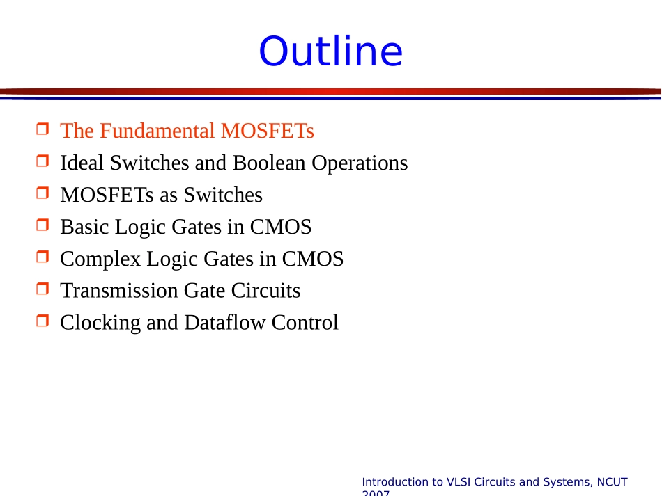
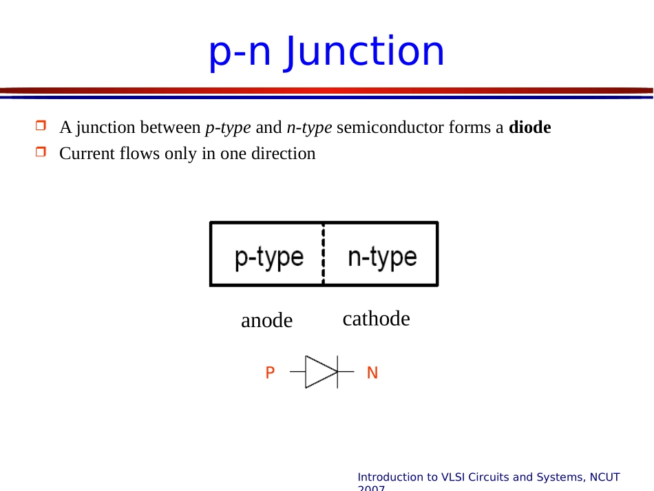
ofElectronicEngineeringNationalChin-YiUniversityofTechnologyFall2007IntroductiontoVLSICircuitsandSystems,NCUT2007OutlineTheFundamentalMOSFETsIdealSwitchesandBooleanOperationsMOSFETsasSwitchesBasicLogicGatesinCMOSComplexLogicGatesinCMOSTransmissionGateCircuitsClockingandDataflowControlIntroductiontoVLSICircuitsandSystems,NCUT2007p-nJunctionAjunctionbetweenp-typeandn-typesemiconductorformsadiodeCurrentflowsonlyinonedirectionanodecathodePNIntroductiontoVLSICircuitsandSystems,NCUT2007nMOSTransistorFourterminals:gate(G),source(S),drain(D),body(B)Gate–oxide–bodystacklookslikeacapacitor»Gateandbodyareconductors»SiO2(oxide)isaverygoodinsulator»Calledmetal–oxide–semiconductor(MOS)capacitor»EventhoughgateisnolongermadeofmetalIntroductiontoVLSICircuitsandSystems,NCUT2007nMOSOperation(1/2)Bodyisusuallytiedtoground(0V)Whenthegateisatalowvoltage»P-typebodyisatlowvoltage»Source-bodyanddrain-bodydiodesareOFF»Nocurrentflows,transistorisOFFIntroductiontoVLSICircuitsandSystems,NCUT2007nMOSOperation(2/2)Whenthegateisatahighvoltage»PositivechargeongateofMOScapacitor»Negativechargeattractedtobody»Invertsachannelundergateton-type»Nowcurrentcanflowthroughn-typesiliconfromsourcethroughchanneltodrain,transistorisONIntroductiontoVLSICircuitsandSystems,NCUT2007pMOSTransistorSimilar,butdopingandvoltagesreversed»Bodytiedtohighvoltage(VDD)»Gate“low”:transistorON»Gate“high”:transistorOFF»BubbleindicatesinvertedbehaviorIntroductiontoVLSICircuitsandSystems,NCUT2007OutlineTheFundamentalMOSFETsIdealSwitchesandBooleanOperationsMOSFETsasSwitchesBasicLogicGatesinCMOSComplexLogicGatesinCMOSTransmissionGateCircuitsClockingandDataflowControlIntroductiontoVLSICircuitsandSystems,NCUT2007IdealSwitches(1/3)CMOSintegratedcircuitsusebi-directionaldevicescalledMOSFETsaslogicswitches»Controlledswitches,e.g,assert-highandassert-lowswitchesAnassert-highswitchisshowinginFigure2.1Figure2.1Behaviorofanassert-highswitch(a)Open(b)ClosedIntroductiontoVLSICircuitsandSystems,NCUT2007IdealSwitches(2/3)g=(a.1).b=(a.1).bg=(a.1)+(b.1)=a+bFigure2.2Series-connectedswitchesFigure2.4Parallel-connectedswitchesIntroductiontoVLSICircuitsandSystems,NCUT2007IdealSwitches(3/3)Figure2.5Anassert-lowswitch(a)Closed(b)OpenFigure2.6Series-connectedcomplementaryswitchesFigure2.7Anassert-lowswitchFigure2.8AMUX-basedNOTgateIntroductiontoVLSICircuitsandSystems,NCUT2007OutlineTheFundamentalMOSFETsIdealSwitchesandBooleanOperationsMOSFETsasSwitchesBasicLogicGatesinCMOSComplexLogicGatesinCMOSTransmissionGateCircuitsClockingandDataflowControlIntroductiontoVLSICircuitsandSystems,NCUT2007MOSFETasSwitchesMOSFET:Metal-Oxide-SemiconductorField-EffectTransistornFET:ann-channelMOSFETthatusesnegativelychargedelectronsforelectricalcurrentflowpFET:ap-channelMOSFETthatusespositivechargesforcurrentflowInmanyways,MOSFETsbehaveliketheidealizedswitchesintroducedintheprevioussectionThevoltageappliedtothegatedeterminesthecurrentflowbetweenthesourceanddrainterminalsFigure2.9SymbolsusedfornFETsandpFETs(a)nFETsymbol(b)pFETsymbolIntroductiontoVLSICircuitsandSystems,NCUT2007MOSFETasSwitchesEarlygenerationsofsiliconMOSlogiccircuitsusedbothposit...