Analog DesignDevice Knowledge1
p+/n- junction and p-/n+ junction, which has a higher breakdown voltage
For a p+/n- junction having NA and ND, what is the approximate function of junction capacitance (Cj) vs
reverse biased voltage (VR)
Draw the cross-section of a CMOS inverter
Draw the parasitic structure on the cross- section
Describe ways to prevent “latch - up”
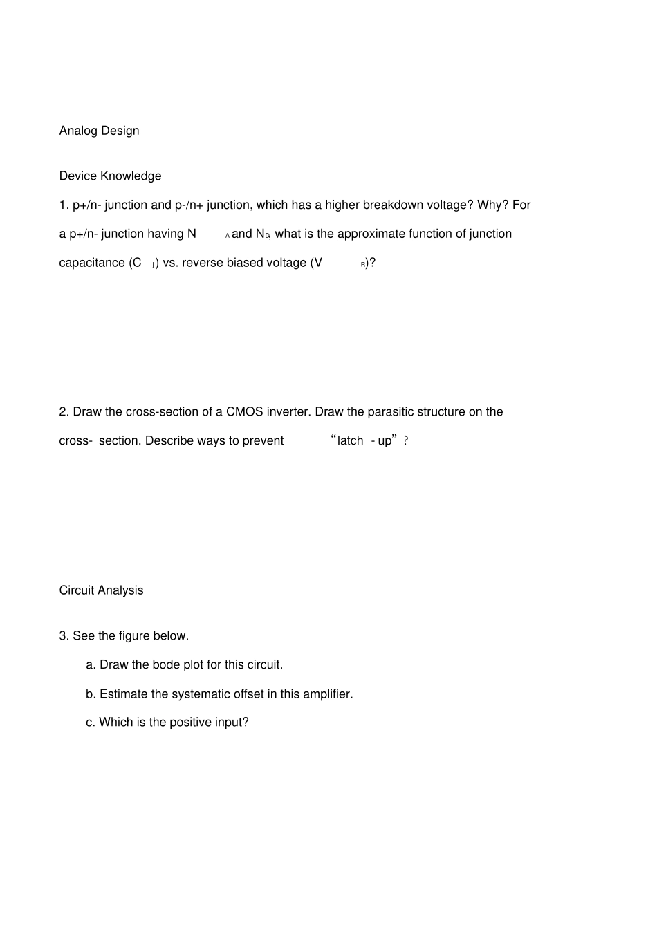
Circuit Analysis3
See the figure below
Draw the bode plot for this circuit
Estimate the systematic offset in this amplifier
Which is the positive input
V CCRO2I+-V INOUTCRO1W/LM 04
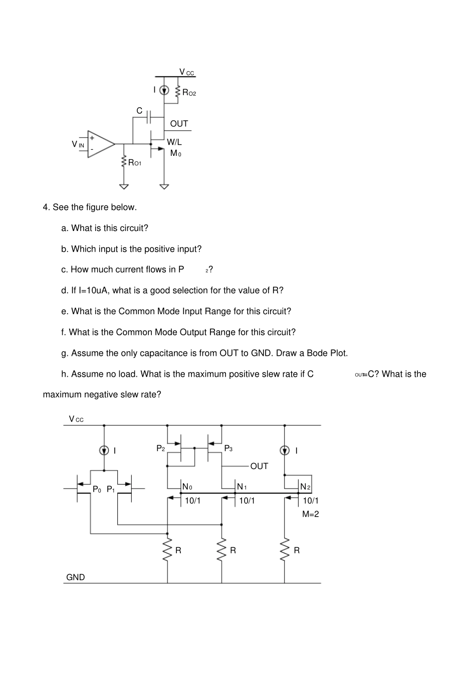
See the figure below
What is this circuit
Which input is the positive input
How much current flows in P2
If I=10uA, what is a good selection for the value of R
What is the Common Mode Input Range for this circuit