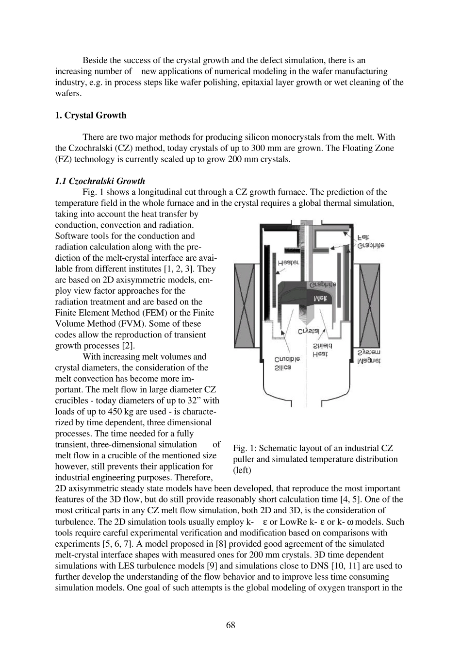
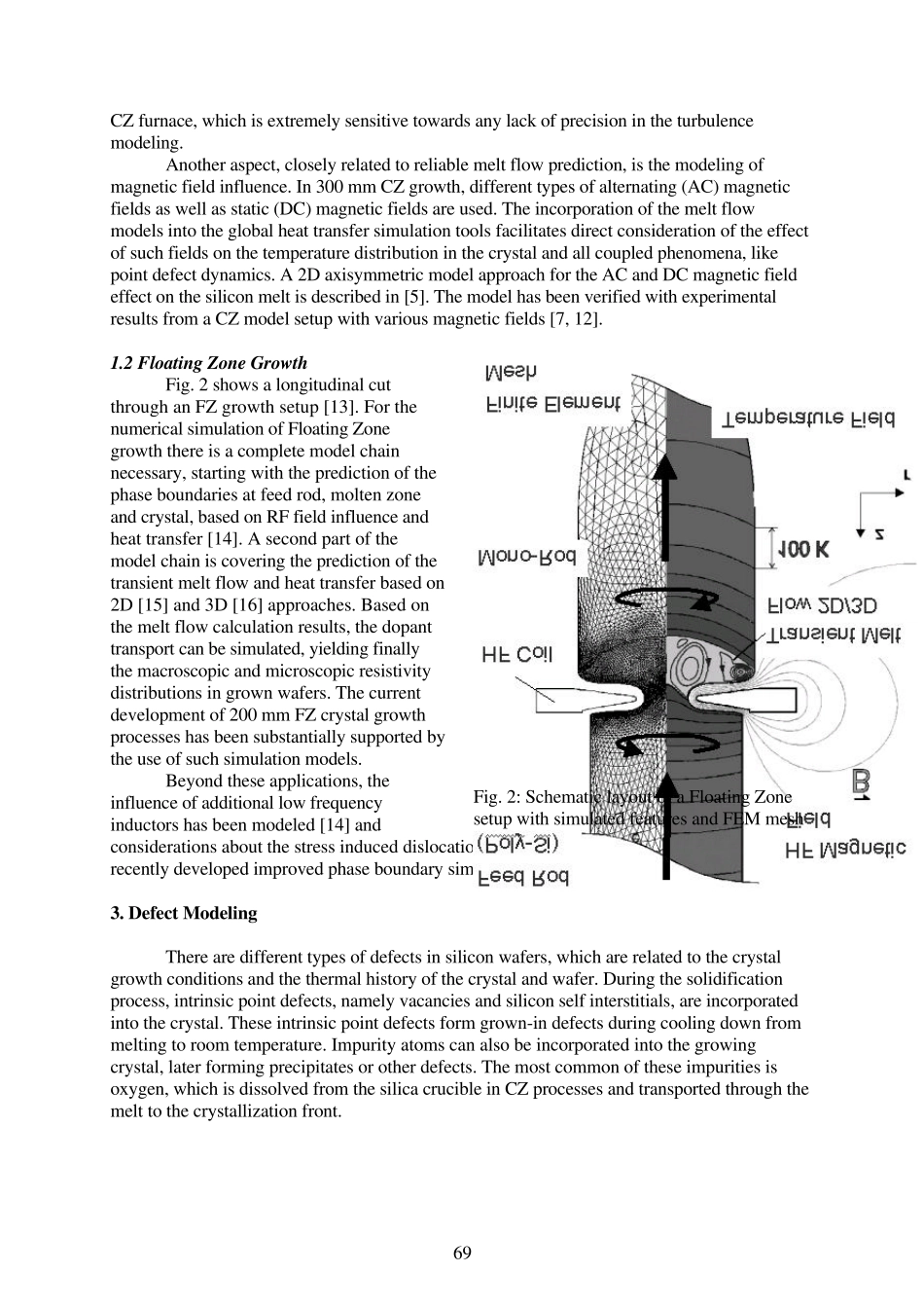
67International Scientific Colloquium Modelling for Electromagnetic Processing Hannover, March 24-26, 2003 Modeling in Industrial Silicon Wafer Manufacturing - From Crystal Growth to Device Processes Th. Wetzel, J. Virbulis Abstract Silicon wafer manufacturing is one of the key processes that determine the yield and the profitability in semiconductor device production. The present paper gives an overview on vari-ous applications for numerical modeling in the wafer manufacturing process. It starts with ther-mal and convection models for the crystal growth process, both by the Czochralski (CZ) and the Floating Zone (FZ) method. Within this field, in particular modeling of electromagnetic field influence on melt flow has become an an indispensable means for the puller design and the process development for both methods. A further chapter is devoted to model approaches for predicting crystal defects, like grown-in voids, self-interstitial aggregates or oxygen precipitates. The defect modeling connect the crystal growth directly to the device manufacturing processes, as crystal defects may be detrimental or beneficial to microelectronic devices, produced on the silicon wafer. A last chapter points briefly to more recent applications of numerical modeling in auxiliary processes, like wafer heat treatment steps, epitaxial growth or wafer cleaning. Introduction During the last five decades, the technology for growing silicon monocrystals from the melt, and the subsequent manufacture of silicon wafers, have become highly developed. The quality, purity and size of today's silicon crystals and wafers have reached an outstanding level. However, it remains time consuming and expensive to develop new processes that meet the crystal...