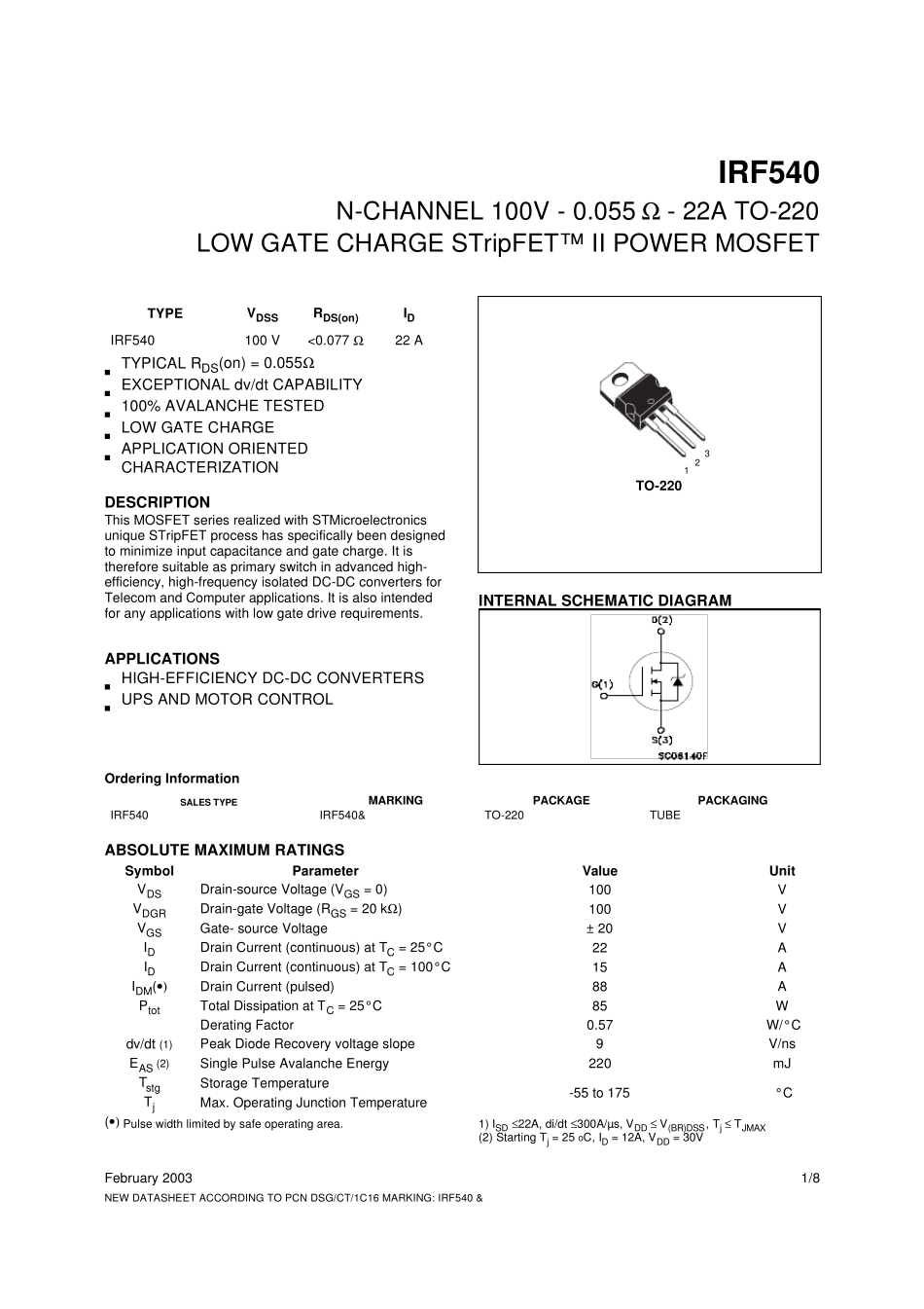
1/8February 2003NEW DATASHEET ACCORDING TO PCN DSG/CT/1C16 MARKING: IRF540 &IRF540N-CHANNEL 100V - 0.055 Ω - 22A TO-220LOW GATE CHARGE STripFET™ II POWER MOSFETs TYPICAL RDS(on) = 0.
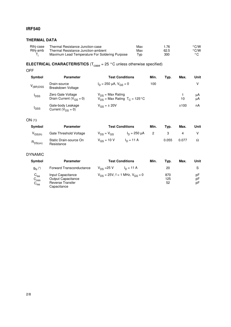
055Ωs EXCEPTIONAL dv/dt CAPABILITYs 100% AVALANCHE TESTEDs LOW GATE CHARGEs APPLICATION ORIENTED CHARACTERIZATIONDESCRIPTIONThis MOSFET series realized with STMicroelectronicsunique STripFET process has specifically been designedto minimize input capacitance and gate charge. It istherefore suitable as primary switch in advanced high-efficiency, high-frequency isolated DC-DC converters forTelecom and Computer applications. It is also intendedfor any applications with low gate drive requirements.APPLICATIONSs HIGH-EFFICIENCY DC-DC CONVERTERSs UPS AND MOTOR CONTROLTYPEVDSSRDS(on)IDIRF540100 V<0.077 Ω22 A123TO-220Ordering InformationABSOLUTE MAXIMUM RATINGS(•) Pulse width limited by safe operating area.1) ISD ≤22A, di/dt ≤300A/µs, VDD ≤ V(BR)DSS, Tj ≤ TJMAX(2) Starting Tj = 25 oC, ID = 12A, VDD = 30VSALES TYPEMARKINGPACKAGEPACKAGINGIRF540IRF540&TO-220TUBESymbolParameterValueUnitVDSDrain-source Voltage (VGS = 0)100VVDGRDrain-gate Voltage (RGS = 20 kΩ)100VVGSGate- source Voltage± 20VIDDrain Current (continuous) at TC = 25°C22AIDDrain Current (continuous) at TC = 100°C15AIDM(•)Drain Current (pulsed)88APtotTotal Dissipation at TC = 25°C85WDerating Factor0.57W/°Cdv/dt (1)Peak Diode Recovery voltage slope9V/nsEAS (2)Single Pulse Avalanche Energy220mJTstgStorage Temperature-55 to 175°CTjMax. Operating Junction TemperatureINTERNAL SCHEMATIC DIAGRAMIRF5402/8THERMAL DATAELECTRICAL CHARACTERISTICS (Tcase = 25 °C unless otherwise specified)OFFON (1)DYNAMICRthj-caseRthj-ambTlThermal Resistance Junction-caseThermal Resistance Junction-ambientMaximum Lead Temperature For Soldering PurposeMaxMaxT...