Integrated Silicon Solution, Inc. — 1-800-379-47741TARGET SPECIFICATIONRev. C05/04/01IS42S16400ISSI®This document contains TARGET SPECIFICATION data. ISSI reserves the right to make changes to its products at any time without notice in order to improve design and supply the bestpossible product. We assume no responsibility for any errors which may appear in this publication. © Copyright 2001, Integrated Silicon Solution, Inc.
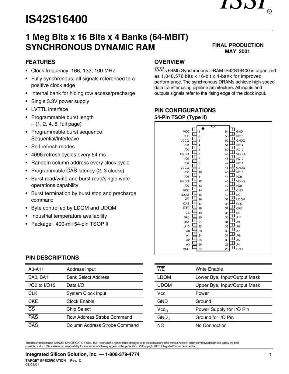
FEATURES• Clock frequency: 166, 133, 100 MHz• Fully synchronous; all signals referenced to apositive clock edge• Internal bank for hiding row access/precharge• Single 3.3V power supply• LVTTL interface• Programmable burst length– (1, 2, 4, 8, full page)• Programmable burst sequence:Sequential/Interleave• Self refresh modes• 4096 refresh cycles every 64 ms• Random column address every clock cycle• Programmable CAS latency (2, 3 clocks)• Burst read/write and burst read/single writeoperations capability• Burst termination by burst stop and prechargecommand• Byte controlled by LDQM and UDQM• Industrial temperature availability• Package: 400-mil 54-pin TSOP IIOVERVIEWIS S I's 64Mb Synchronous DRAM IS42S16400 is organizedas 1,048,576 bits x 16-bit x 4-bank for improvedperformance. The synchronous DRAMs achieve high-speeddata transfer using pipeline architecture. All inputs andoutputs signals refer to the rising edge of the clock input.1 Meg Bits x 16 Bits x 4 Banks (64-MBIT)SYNCHRONOUS DYNAMIC RAMFINAL PRODUCTIONMAY 2001PIN CONFIGURATIONS54-Pin TSOP (Type II)VCCI/O0VCCQI/O1I/O2GNDQI/O3I/O4VCCQI/O5I/O6GNDQI/O7VCCLDQMW ECASRASCSBA0BA1A10A0A1A2A3VCC123456789101112131415161718192021222324252627545352515049484746454443424140393837363534333231302928GNDI/O15GNDQI/O14I/O13VCCQI/O12I/O11GNDQI/O10I/O9VCCQI/O8GNDNCUDQMCLKCKENCA11A9A8A7A6A5A4G...