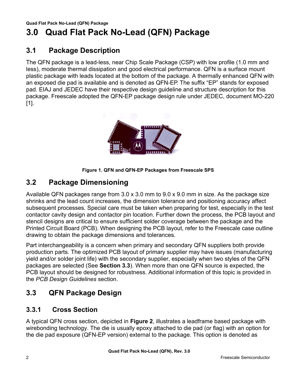
© Freescale Semiconductor, Inc., 2005. All rights reserved. Freescale SemiconductorApplication NoteAN1902Rev. 3.0, 12/20051.0PurposeThis document provides guidelines for Printed Circuit Board (PCB) design and assembly. Package performance such as: MSL rating, board level reliability, electrical parasitic and thermal resistance data are included as reference.2.0ScopeThe Application Note is written generically to encompass various Quad Flat Pack No-lead (QFN) packages assembled internally and externally. It should be noted that device specific information is not provided. This document serves only as a guideline to help develop a user specific solution. Actual experience and development efforts are still required to optimize the process per individual device requirements and practices.The document combines information from two separate studies. This is the first data consolidation attempt. When recommendation varies between the two studies, both views are provided and the source noted. Quad Flat Pack No-Lead (QFN)Contents 1.0 Purpose . . . . . . . . . . . . . . . . . . . . . . . . . . . . . . . .1 2.0 Scope . . . . . . . . . . . . . . . . . . . . . . . . . . . . . . . . . .1 3.0 Quad Flat Pack No-Lead (QFN) Package . . . . .2 3.1 Package Description. . . . . . . . . . . . . . . . . . . . . .2 3.2 Package Dimensioning. . . . . . . . . . . . . . . . . . . .2 3.3 QFN Package Design . . . . . . . . . . . . . . . . . . . . .2 3.4 Process Flow . . . . . . . . . . . . . . . . . . . . . . . . . . . .4 4.0 Printed Circuit Board (PCB) Level Guidelines .5 4.1 PCB Design Guideline . . . . . . . . . . . . . . . . . . . .5 4.2 St...