DDR 时序测试方法 1. 参考文献: RS –Springdale-G/P/PE MCH external design specification(EDS) addendum (number:780) 2. 测试目的: 在P4D 项目(Springdale-G/PE)中, 主要看System ddr Data 和Strobe 信号的时序质量是否满足规范要求. 3. 
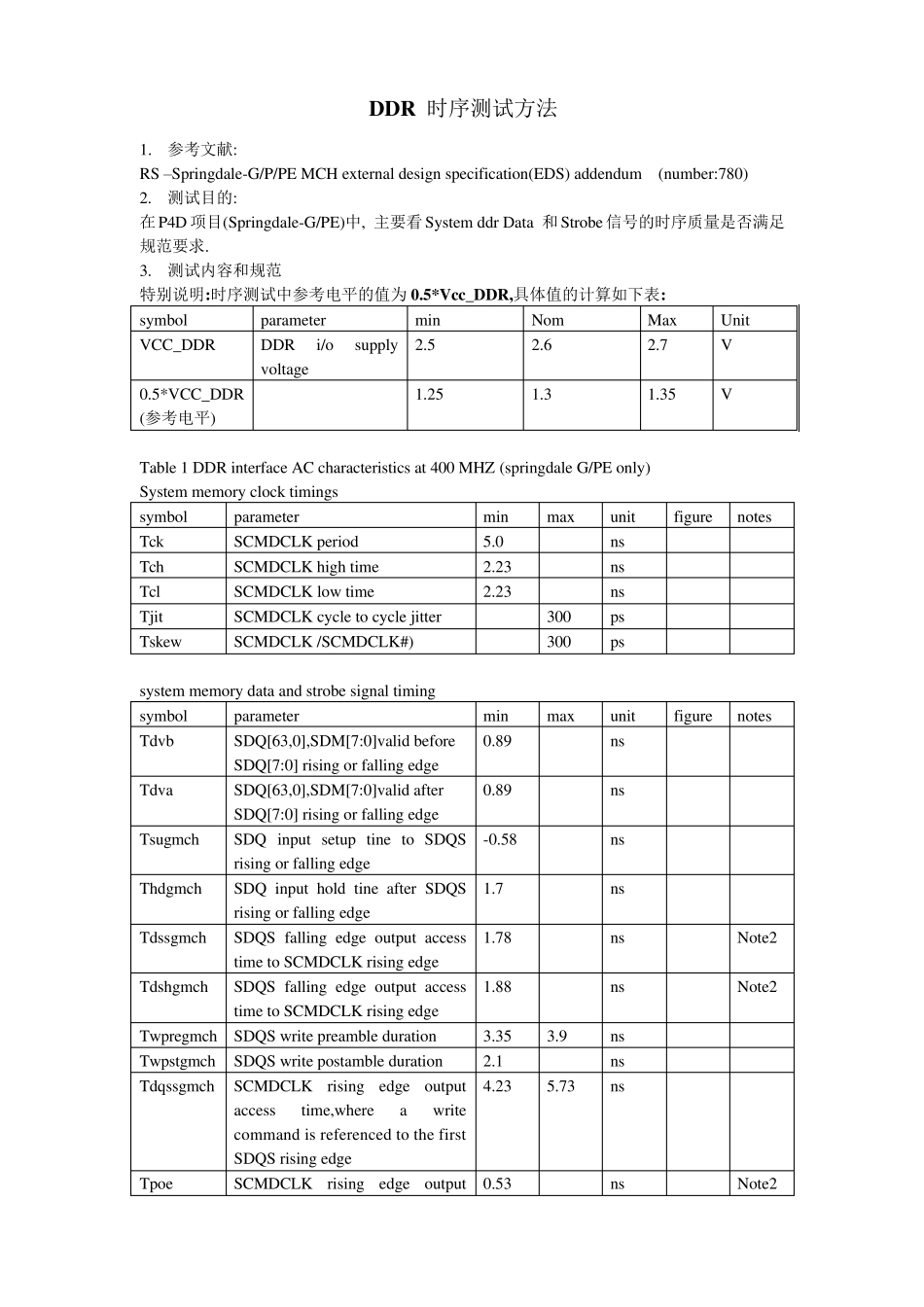
测试内容和规范 特别说明:时序测试中参考电平的值为0.5*Vcc_DDR,具体值的计算如下表: symbol parameter min Nom Max Unit VCC_DDR DDR i/o supply voltage 2.5 2.6 2.7 V 0.5*VCC_DDR (参考电平) 1.25 1.3 1.35 V Table 1 DDR interface AC characteristics at 400 MHZ (springdale G/PE only) System memory clock timings symbol parameter min max unit figure notes Tck SCMDCLK period 5.0 ns Tch SCMDCLK high time 2.23 ns Tcl SCMDCLK low time 2.23 ns Tjit SCMDCLK cycle to cycle jitter 300 ps Tskew SCMDCLK /SCMDCLK#) 300 ps system memory data and strobe signal timing symbol parameter min max unit figure notes Tdvb SDQ[63,0],SDM[7:0]valid before SDQ[7:0] rising or falling edge 0.89 ns Tdva SDQ[63,0],SDM[7:0]valid after SDQ[7:0] rising or falling edge 0.89 ns Tsugmch SDQ input setup tine to SDQS rising or falling edge -0.58 ns Thdgmch SDQ input hold tine after SDQS rising or falling edge 1.7 ns Tdssgmch SDQS falling edge output access time to SCMDCLK rising edge 1.78 ns Note2 Tdshgmch SDQS falling edge output access time to SCMDCLK rising edge 1.88 ns Note2 Twpregmch SDQS write preamble duration 3.35 3.9 ns Twpstgmch SDQS write postamble duration 2.1 ns Tdqssgmch SCMDCLK rising edge output access time,where a write command is referenced to the first SDQS rising edge 4.23 5.73 ns Tpoe SCMDCLK rising edge output 0.53 ns Note2 access time,w here a w rite command is referenced to the SDQS preamble falling edge Note2:SCMDCLK 上 升 沿 参 考 SCMDCLK 上 升 沿 和 SCMDCLK# 下 降 沿 的 交 叉 点 ; SCMDCLK 下降沿参考 SCMDC...