This is the first of a multi-part series, to introduce FinFET technology to SemiWiki readers. These articles will highlight the technology's key characteristics, and describe some of the advantages, disadvantages, and challenges associated with this transition. Topics in this series will include FinFET fabrication, modeling, and the resulting impact upon existing EDA tools and flows. (And, of course, feedback from SemiWiki readers will certainly help influence subsequent topics, as well.) Scaling of planar FET's has continued to provide performance, power, and circuit density improvements, up to the 22/20nm process node. Although active research on FinFET devices has been ongoing for more than a decade, their use by a production fab has only recently gained adoption
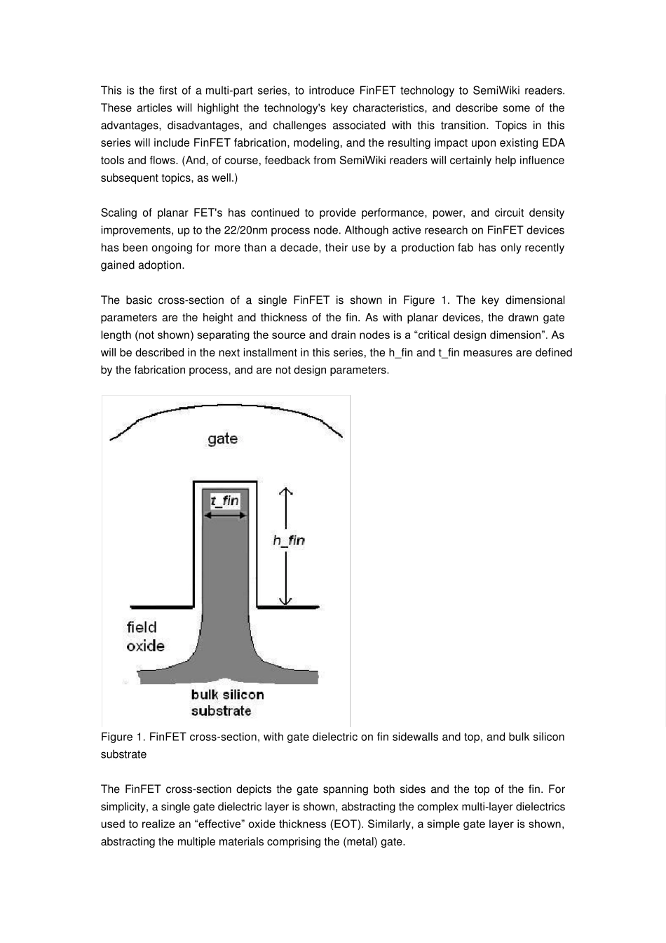
. The basic cross-section of a single FinFET is shown in Figure 1. The key dimensional parameters are the height and thickness of the fin. As with planar devices, the drawn gate length (not shown) separating the source and drain nodes is a “critical design dimension”. As will be described in the next installment in this series, the h_fin and t_fin measures are defined by the fabrication process, and are not design parameters. Figure 1. FinFET cross-section, with gate dielectric on fin sidewalls and top, and bulk silicon substrate The FinFET cross-section depicts the gate spanning both sides and the top of the fin. For simplicity, a single gate dielectric layer is shown, abstracting the complex multi-layer dielectrics used to realize an “effective” oxide thickness (EOT). Similarly, a simple gate layer is shown, abstracting the multiple materials comprising the (metal) gate. In the research literature, FinFET's have also been fabricated with...