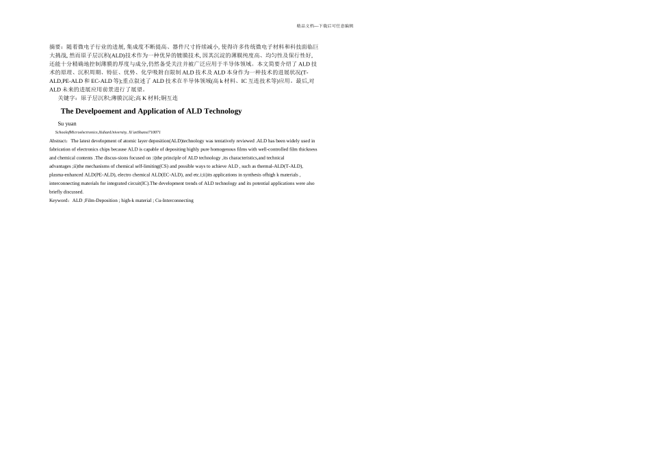
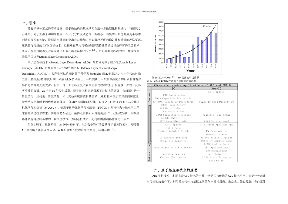
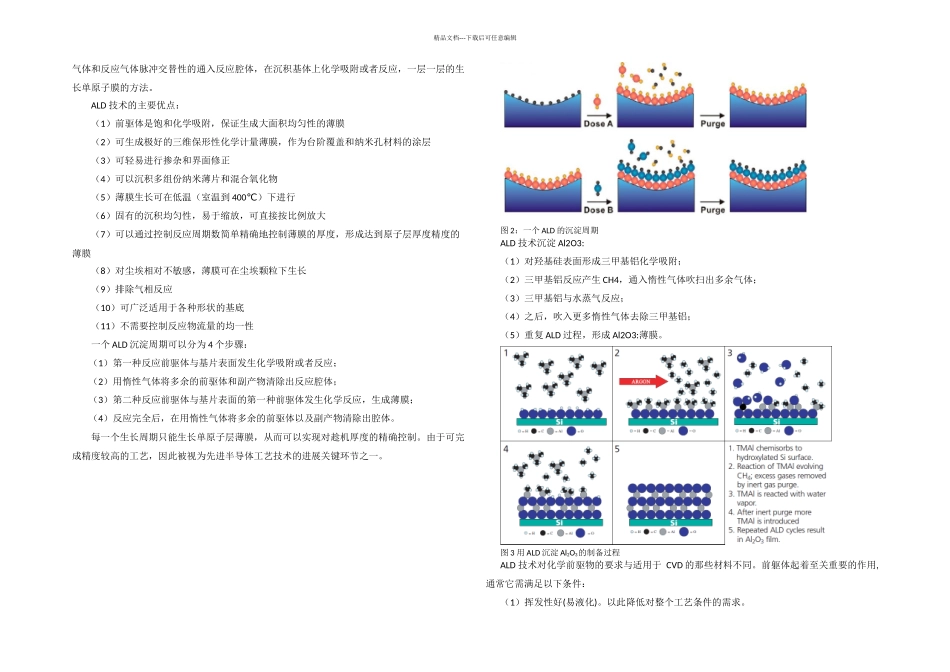
精品文档---下载后可任意编辑摘要:随着微电子行业的进展, 集成度不断提高、器件尺寸持续减小, 使得许多传统微电子材料和科技面临巨大挑战, 然而原子层沉积(ALD)技术作为一种优异的镀膜技术, 因其沉淀的薄膜纯度高、均匀性及保行性好, 还能十分精确地控制薄膜的厚度与成分,仍然备受关注并被广泛应用于半导体领域
本文简要介绍了 ALD 技术的原理、沉积周期、特征、优势、化学吸附自限制 ALD 技术及 ALD 本身作为一种技术的进展状况(T-ALD,PE-ALD 和 EC-ALD 等);重点叙述了 ALD 技术在半导体领域(高 k 材料、IC 互连技术等)应用
最后,对ALD 未来的进展应用前景进行了展望
关键字:原子层沉积;薄膜沉淀;高 K 材料;铜互连The Develpoement and Application of ALD TechnologySu yuanSchoolofMicroelectronics,XidianUniversity, Xi’anShanxi710071Abstract:The latest development of atomic layer deposition(ALD)technology was tentatively reviewed
ALD has been widely used in fabrication of electronics chips because ALD is capable of depositing highly pure homogenous films with well-controlled film thickness and chemical contents
The discus-sions focused on :i)the principle of ALD technology ,its