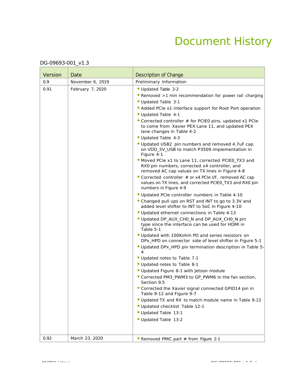
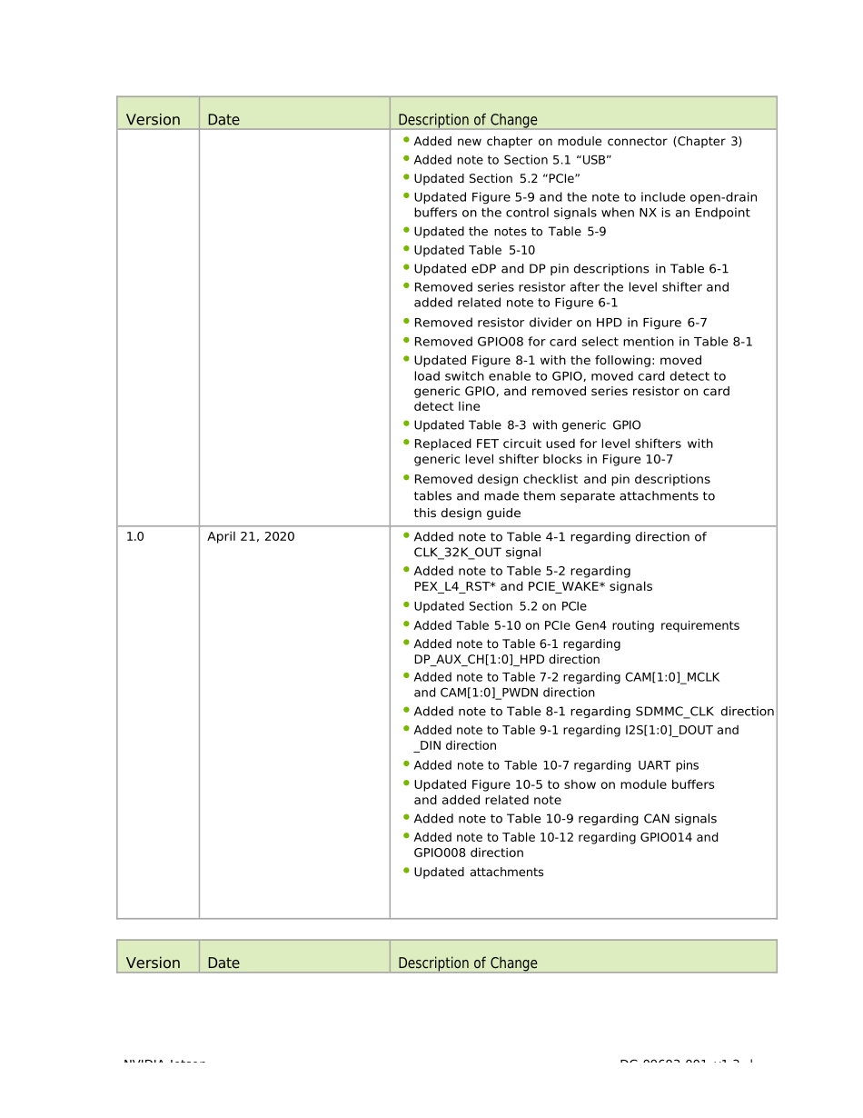
DG-09693-001_v1.3 | November 2020NVIDIA Jetson Xavier NXDesign GuideNVIDIA Jetson DG-09693-001_v1.3 | Document HistoryDG-09693-001_v1.3VersionDateDescription of Change0.9November 6, 2019Preliminary Information0.91February 7, 2020 Updated Table 2-2 Removed >1 min recommendation for power rail charging Updated Table 3-1 Added PCIe x1 interface support for Root Port operation Updated Table 4-1 Corrected controller # for PCIE0 pins, updated x1 PCIe to come from Xavier PEX Lane 11, and updated PEX lane changes in Table 4-2 Updated Table 4-3 Updated USB2 pin numbers and removed 4.7uF cap on VDD_5V_USB to match P3509 implementation in Figure 4-1 Moved PCIe x1 to Lane 11, corrected PCIE0_TX3 and RX0 pin numbers, corrected x4 controller, and removed AC cap values on TX lines in Figure 4-8 Corrected controller # or x4 PCIe I/F, removed AC cap values on TX lines, and corrected PCIE0_TX3 and RX0 pin numbers in Figure 4-9 Updated PCIe controller numbers in Table 4-10 Changed pull ups on RST and INT to go to 3.3V and added level shifter to INT to SoC in Figure 4-10 Updated ethernet connections in Table 4-13 Updated DP_AUX_CH0_N and DP_AUX_CH0_N pin type since the interface can be used for HDMI in Table 5-1 Updated with 100Kohm PD and series resistors on DPx_HPD on connector side of level shifter in Figure 5-1 Updated DPx_HPD pin termination description in Table 5-4 Updated notes to Table 7-1 Updated notes to Table 8-1 Updated Figure 8-1 with Jetson module Corrected PM3_PWM3 to GP_PWM6 in the fan section, Section 9.5 Corrected the Xavier signal connected GPIO14 pin in Table 9-12 and Figure 9-7 Updated TX and RX to match module name in Table 9-13 Updated checklist Tabl...