Grounding of Mixed Signal PCBsA question that I hear often is: How do I prevent digital logic ground currents from contaminating my low level analog circuitry? This is a good question without a simple answer. Most A/D converter manufacturer's data books and application notes provide little if any useful information on the subject. If they do provide information, it is usually only applicable to a simple system containing only one A/D converter. Some people suggest splitting the ground plane in order to isolate the digital ground currents from the analog ground currents. Although the split plane approach can be made to work, it has many potential problems especially in large complicated systems. Can you list some of these problems? 
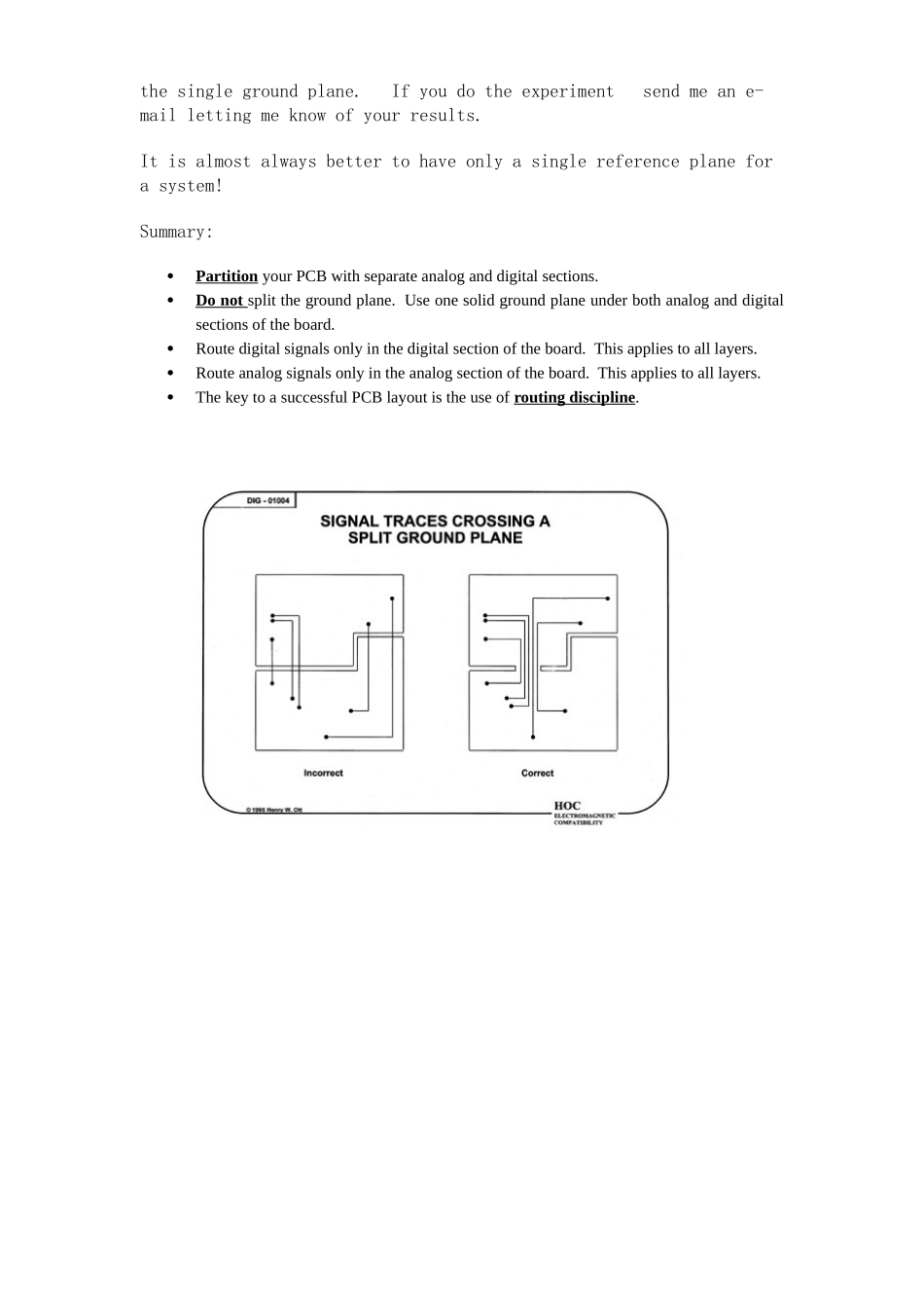
One of the major ones is that you can not route a trace over the split in the plane (see Tech Tip Slots in Ground Planes).It is always better to have only a single reference plane for a system. If you do split the ground plane and run traces across the split (left hand figure below), there will be no return path near the trace and the current will have to flow in a big loop. Current flowing in big loops produce radiation and high ground inductance. If you must split the ground plane and run traces across the split, you should do it as shown in the right hand figure below. By connecting the planes together at one point (a bridge) and routing all the traces so that they cross at this bridge point, you will have provided a return path for the current directly underneath each of the traces (hence a very small loop area). High frequency digital ground return currents want to return directly underneath the signal trace. This is the lowest impedance (low...