SymbolVDSVGSIDMTJ, TSTGSymbolTypMax659085125RθJL4360Junction and Storage Temperature RangeAPD°C1.41-55 to 150TA=70°CID-4.2-3.
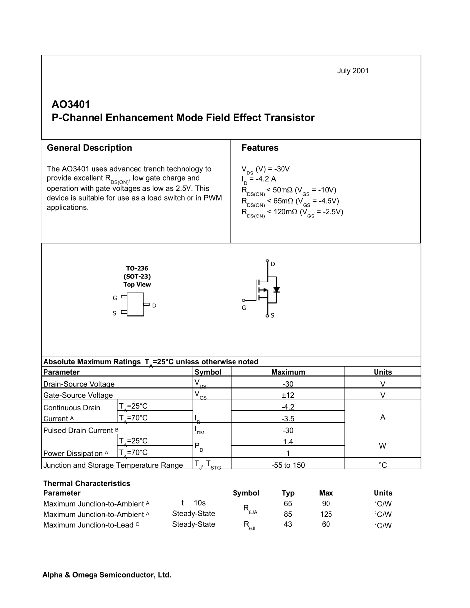
5-30Pulsed Drain Current BPower Dissipation ATA=25°CContinuous Drain Current AMaximumUnitsParameterTA=25°CTA=70°CAbsolute Maximum Ratings TA=25°C unless otherwise notedVV±12Gate-Source VoltageDrain-Source Voltage-30°C/WMaximum Junction-to-Ambient ASteady-State°C/WWMaximum Junction-to-Lead CSteady-State°C/WThermal CharacteristicsParameterUnitsMaximum Junction-to-Ambient At ≤ 10sRθJAAO3401P-Channel Enhancement Mode Field Effect TransistorJuly 2001FeaturesVDS (V) = -30VID = -4.2 ARDS(ON) < 50mΩ (VGS = -10V)RDS(ON) < 65mΩ (VGS = -4.5V)RDS(ON) < 120mΩ (VGS = -2.5V)General DescriptionThe AO3401 uses advanced trench technology to provide excellent RDS(ON), low gate charge and operation with gate voltages as low as 2.5V. This device is suitable for use as a load switch or in PWM applications.SGDTO-236(SOT-23)Top ViewG D S Alpha & Omega Semiconductor, Ltd.AO3401SymbolMinTypMaxUnitsBVDSS-30V-1TJ=55°C-5IGSS±100nAVGS(th)-0.7-1-1.3VID(ON)-25A4250TJ=125°C755365mΩ80120mΩgFS711SVSD-0.75-1VIS-2.2ACiss954pFCoss115pFCrss77pFRg6ΩQg9.4nCQgs2nCQgd3nCtD(on)6.3nstr3.2nstD(off)38.2nstf12nstrr20.2nsQrr11.2nCBody Diode Reverse Recovery TimeBody Diode Reverse Recovery Charge IF=-4A, dI/dt=100A/µsDrain-Source Breakdown VoltageOn state drain currentID=-250µA, VGS=0V VGS=-2.5V, ID=-1A VGS=-4.5V, VDS=-5VVGS=-10V, ID=-4.2A Reverse Transfer CapacitanceElectrical Characteristics (TJ=25°C unless otherwise noted)STATIC PARAMETERSParameterConditionsIDSSµAGate Threshold VoltageVDS=VGS ID=-250µAVDS=-24V, VGS=0V VDS=0V, VGS=±12VZero Gate Voltage Drain CurrentGate-Body leakage currentRDS(ON)Static Drain-Source On-ResistanceForward TransconductanceDiode Forward VoltagemΩVGS=-4.5V, ID=-4A IS=-1A,VGS=0VVDS=...