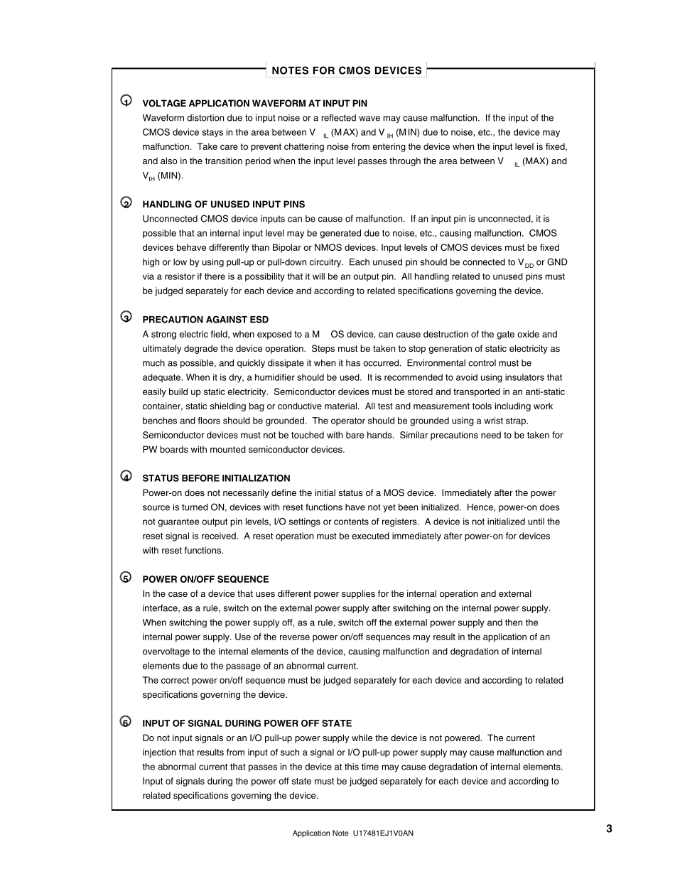
Docu ment No. U17481EJ1V0AN00 (1st edition) Date Pu blished September 2005 N CP(K) Printed in Japan Single-Phase Induction Motor Control by µPD78F0714 Two-Phase Sine Wave Inverter Drive via V/f Control 2005 µPD78F0714 Application Note Application Note U17481EJ1V0AN 2 [MEMO] Application Note U17481EJ1V0AN 31234VOLTAGE APPLICATION WAVEFORM AT INPUT PINWaveform distortion due to input noise or a reflected wave may cause malfunction. If the input of the CMOS device stays in the area between VIL (MAX) and V IH (MIN) due to noise, etc., the device may malfunction. Take care to prevent chattering noise from entering the device when the input level is fixed, and also in the transition period when the input level passes through the area between VIL (MAX) and VIH (MIN).HANDLING OF UNUSED INPUT PINSUnconnected CMOS device inputs can be cause of malfunction. If an input pin is unconnected, it is possible that an internal input level may be generated due to noise, etc., causing malfunction. CMOS devices behave differently than Bipolar or NMOS devices. Input levels of CMOS devices must be fixed high or low by using pull-up or pull-down circuitry. Each unused pin should be connected to VDD or GND via a resistor if there is a possibility that it will be an output pin. All handling related to unused pins must be judged separately for each device and according to related specifications governing the device.PRECAUTION AGAINST ESD A strong electric field, when exposed to a MOS device, can cause destruction of the gate oxide and ultimately degrade the device operation. Steps must be taken to stop generation of static electricity as much as possible, and quickly dissipate it when it has occurred. Environmental ...