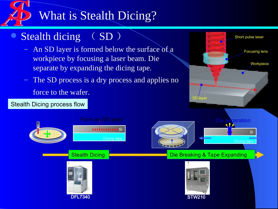
StealthDicingProcessIntroductionWhatisStealthDicing?Stealthdicing(SD)–AnSDlayerisformedbelowthesurfaceofaworkpiecebyfocusingalaserbeam.Dieseparatebyexpandingthedicingtape.–TheSDprocessisadryprocessandappliesnoforcetothewafer.
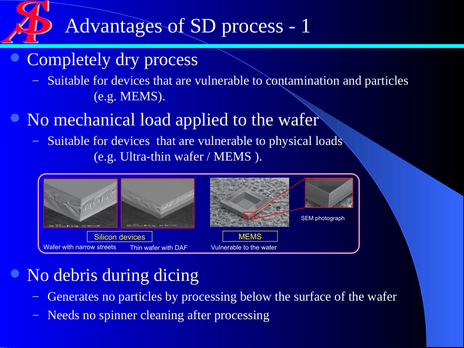
ShortpulselaserFocusinglensWorkpieceSDlayerStealthDicingprocessflowStealthDicingDieBreaking&TapeExpandingFormanSDlayerDFL7340STW210DieseparationDicingtapeSiDicingtapeSiCompletelydryprocess–Suitablefordevicesthatarevulnerabletocontaminationandparticles(e.g.MEMS).Nomechanicalloadappliedtothewafer–Suitablefordevicesthatarevulnerabletophysicalloads(e.g.Ultra-thinwafer/MEMS).Nodebrisduringdicing–Generatesnoparticlesbyprocessingbelowthesurfaceofthewafer–NeedsnospinnercleaningafterprocessingWaferwithnarrowstreetsMEMSVulnerabletothewaterSilicondevicesThinwaferwithDAFSEMphotographAdvantagesofSDprocess-1Afterexpanding•Kerfwidth:0um•Chipping:0um(Afewmicrometersofmeandermightoccurduringtheseparationprocess.)200mBeforeexpanding20mExtremelythinkerf–GreatlycontributestostreetreductionbecausethekerfwidthcanbemadeextremelythinAdvantagesofSDprocess-2-Thenumberofpasses1-Feedspeed300mm/s-Diesize5×5mmSi:Thickness100μm50m55μmSDlayer-Thenumberofpasses7*-Feedspeed300mm/s-Diesize5×5mm*Oneextrapassperstreetisneededtomap(measure+record)theworkpiecesurface100mSi:Thickness300μm40μmSDlayerDicingwithoutfrontorbacksidechipping–BycontrollingthepositionoftheSDlayer,thedamagetobothsurfacescanbereducedAdvantagesofSDprocess-3T:WaferthicknessW:StreetwidthorclearwidthTSiIncidentpointLimitationofstreetwidthW>0.4xTWLimitationsoftheSDprocess–MetalinthestreetAlasercannotpenetratethemetal–Films(e.g.SiO2,SiN,polyimide)Theyarepermeablematerials,butcanbeprocessed–Streetwidth/thicknessratioClearwidthisdeterminedbythethicknessofthewaferLimitationoftheexpandprocess–ThickmetalItmaybedifficulttoseparateallofthemetal–Diesizeof1mmsquareorlessAseparationprocesswillbeneededforsmalldieLimitationsofSDprocessSDsolutionofShin’AuShin’AuwillprovidethespecialSDsolution,whichistobeprocessedfrombacksideofworkpiece.Ifso,theSDprocesswon’tbelimitedbythestreetwidth&metalinthestreet.Shin’AuSDprocessflowStealthDicingDieBreaking,Tapeexpanding&TransferringFormanSDlayerDFL7340STW210DieseparationDicingtapeSiPatternsideSiliconsideTapemountfromwaferbacksideTapemountSiliconsidePatternsideQualityControl-ParticlesRequirednoparticleonthepad-KerflinearityKerfoffsetdistancelessthan5um-NodoubledieoccurredduringwaferbreakingConcern&Discussion-NeedbumpinglayouttocheckifanyimpacttoSDprocess-Dummywafer/EngineeringqualprocessrequiredCapacityCapacity(Pcs/month)Laser-Saw2,000ShinAuSemiconductorShinAuSemiconductor