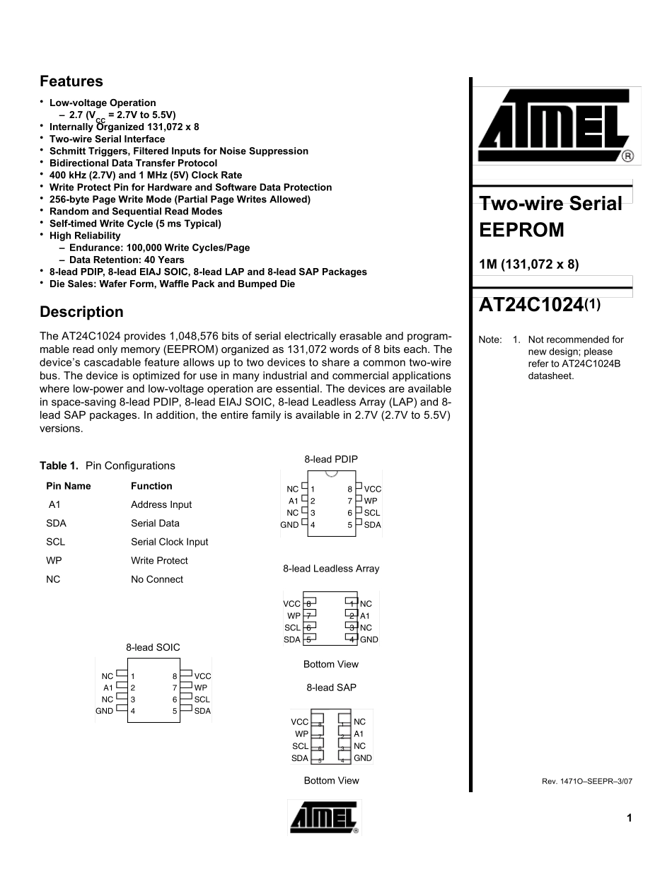
1Features• Low-voltage Operation– 2.7 (VCC = 2.7V to 5.5V)• Internally Organized 131,072 x 8• Two-wire Serial Interface• Schmitt Triggers, Filtered Inputs for Noise Suppression• Bidirectional Data Transfer Protocol• 400 kHz (2.7V) and 1 MHz (5V) Clock Rate• Write Protect Pin for Hardware and Software Data Protection• 256-byte Page Write Mode (Partial Page Writes Allowed)• Random and Sequential Read Modes• Self-timed Write Cycle (5 ms Typical)• High Reliability– Endurance: 100,000 Write Cycles/Page– Data Retention: 40 Years• 8-lead PDIP, 8-lead EIAJ SOIC, 8-lead LAP and 8-lead SAP Packages• Die Sales: Wafer Form, Waffle Pack and Bumped DieDescriptionThe AT24C1024 provides 1,048,576 bits of serial electrically erasable and program-mable read only memory (EEPROM) organized as 131,072 words of 8 bits each. Thedevice’s cascadable feature allows up to two devices to share a common two-wirebus. The device is optimized for use in many industrial and commercial applicationswhere low-power and low-voltage operation are essential. The devices are availablein space-saving 8-lead PDIP, 8-lead EIAJ SOIC, 8-lead Leadless Array (LAP) and 8-lead SAP packages. In addition, the entire family is available in 2.7V (2.7V to 5.5V)versions. Table 1. Pin ConfigurationsPin NameFunction A1Address InputSDASerial DataSCLSerial Clock InputWPWrite ProtectNCNo ConnectTwo-wire Serial EEPROM1M (131,072 x 8)AT24C1024(1) Note:1. Not recommended fornew design; pleaserefer to AT24C1024Bdatasheet. Rev. 1471O– SEEPR– 3/078-lead PDIP12348765NCA1NCGNDVCCW PSCLSDA8-lead Leadless Array Bottom View12348765VCCW PSCLSDANCA1NCGND8-lead SOIC12348765NCA1NCGNDVCCW PSCLSDA8-lead SAPBottom ViewVCCW PSCLSDANCA1NCGND123487652AT24C10241471O–SEEPR–3/07Figure 1. Block DiagramAbsolut...