Rev. 1.
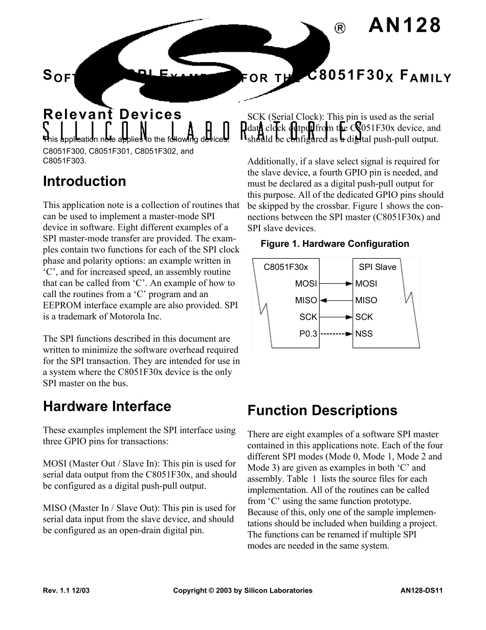
1 12/03Copyright © 2003 by Silicon LaboratoriesAN128-DS11AN128SOFTWARE SPI EXAMPLES FOR THE C8051F30X FAMILYRelevant DevicesThis application note applies to the following devices:C8051F300, C8051F301, C8051F302, and C8051F303.IntroductionThis application note is a collection of routines thatcan be used to implement a master-mode SPIdevice in software. Eight different examples of aSPI master-mode transfer are provided. The exam-ples contain two functions for each of the SPI clockphase and polarity options: an example written in‘C’, and for increased speed, an assembly routinethat can be called from ‘C’. An example of how tocall the routines from a ‘C’ program and anEEPROM interface example are also provided. SPIis a trademark of Motorola Inc.The SPI functions described in this document arewritten to minimize the software overhead requiredfor the SPI transaction. They are intended for use ina system where the C8051F30x device is the onlySPI master on the bus.Hardware InterfaceThese examples implement the SPI interface usingthree GPIO pins for transactions:MOSI (Master Out / Slave In): This pin is used forserial data output from the C8051F30x, and shouldbe configured as a digital push-pull output.MISO (Master In / Slave Out): This pin is used forserial data input from the slave device, and shouldbe configured as an open-drain digital pin.SCK (Serial Clock): This pin is used as the serialdata clock output from the C8051F30x device, andshould be configured as a digital push-pull output.Additionally, if a slave select signal is required forthe slave device, a fourth GPIO pin is needed, andmust be declared as a digital push-pull output forthis purpose. All of the dedicated GPIO pins shouldbe skipped by th...