在fpga 芯片中支持不同io 电平标准 2008-06-06 15:15:39| 分类: FPGA AND DSP | 标签: |字号大中小 订阅 I/O Banking Some of the I/O standards described above require VCCO and/or VREF voltages
These voltages are externally supplied and connected to device pins that serve groups of IOBs, called banks
Consequently, restrictions exist about which I/O standards can be combined within a given bank
Eight I/O banks result from separating each edge of the FPGA into two banks (see Figure 3)
The pinout tables show the bank affiliation of each I/O (see Pinout Tables, Module 4)
Each bank has multiple VCCO pins which must be connected to the same voltage
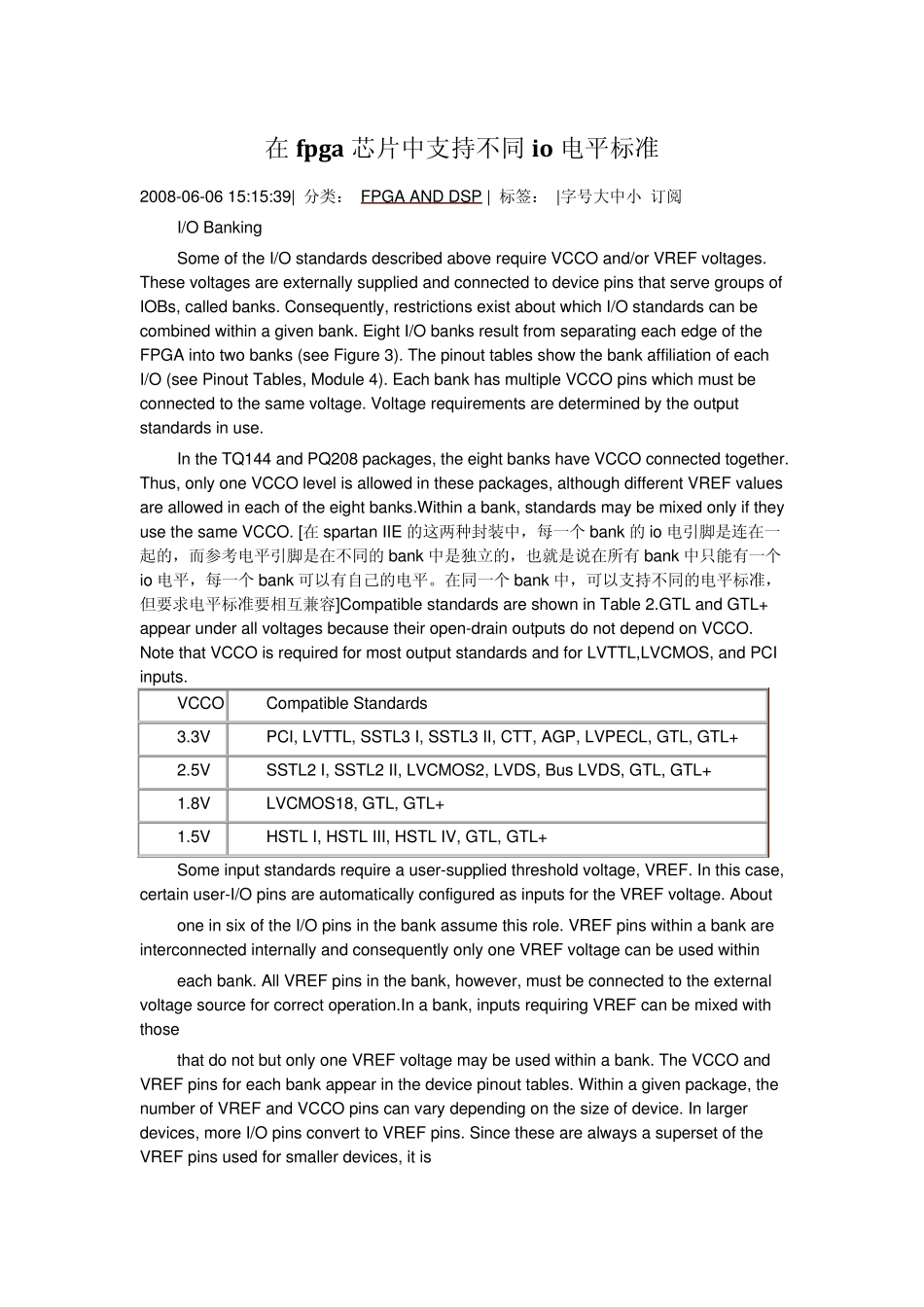
Voltage requirements are determined by the output standards in use
In the TQ144 and PQ208 packages, the eight banks have VCCO connected together
Thus, only one VCCO level i