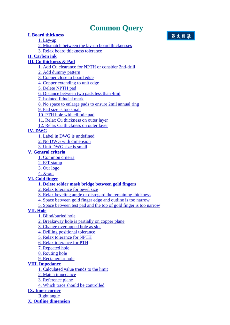
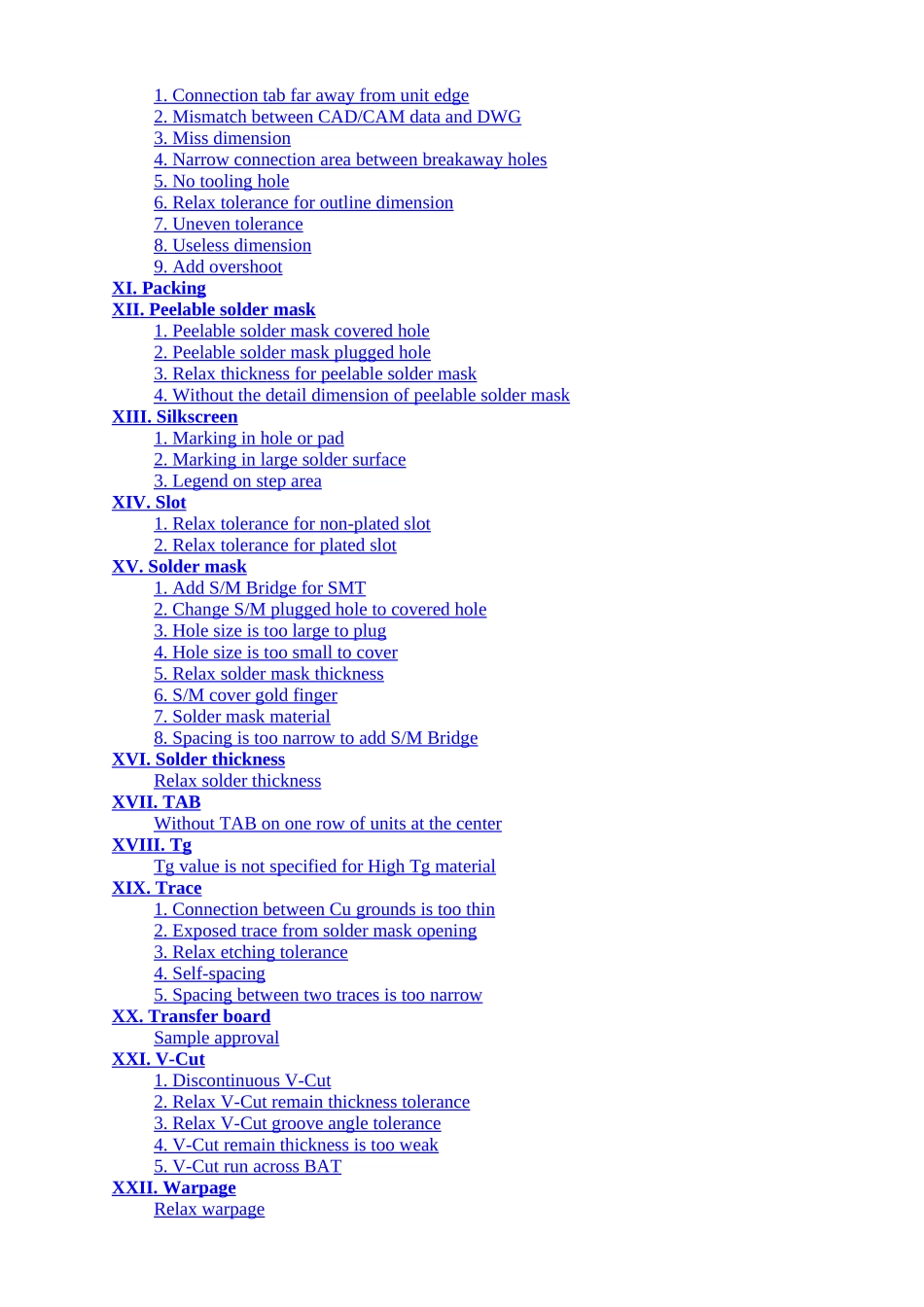
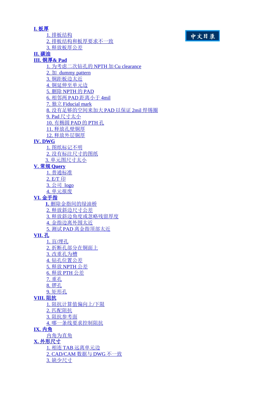
Common Query I . Board thick n ess 1. Lay-up2. Mismatch between t h e lay-up board thicknesses 3. Relax board thic k ness tolerance II . Car b on i n k III . Cu thickness & Pad 1. Add Cu clearance for NPTH or consider 2nd-drill2. Add dummy pattern3. Copper close to board edge4. Copper extending to unit edge5. De l ete NPTH p ad 6. Distance b etw e en two pads less than 4mil 7. Isolated fiducial mark8. No space to enlarge pads to ensure 2mil annual ring9. Pad size is too small10. PTH hole with elliptic pad11. Relax Cu thickness on outer layer12. Relax Cu thickness on outer layerIV . DWG 1. Label in DWG is undefined2. No DWG with dimension 3. Unit DWG size is smallV . General criteria 1. Common criteria2. E/T stamp3. Our logo4. X -out VI . Gold finger 1. Delete solder mask bridge between gold fingers2. Relax tol e rance for bevel size 3. Relax beveling angle or disregard the remaining thickness4. Space between gold finger edge and outline is too narrow5. Space between test pad and the top of gold finger is too narrowVII . Hole 1. Blind/buried hole2. Breakaway hole is partially on copper plane3. Change overlapped hole as slot4. Drilling positional tolerance5. Relax tolerance for NPTH6. Relax tolerance for PTH7. Repeated hole8. Routing hole9. Rectangular holeVIII . Impedance 1. Calculated value trends to the limit2. Match impedance3. Reference plane4. Which trace should be controlledIX . Inner corner Right a n gle X . Outline dimension 1. Connection tab far away from unit edge2. Mismatch between CAD/CAM data and DWG3. Miss dimension4. Narrow connection area between breakaway holes5. No tooling hole6. Relax tolerance for outline dimension7. Uneven tolerance8. Useless dimensio n 9....