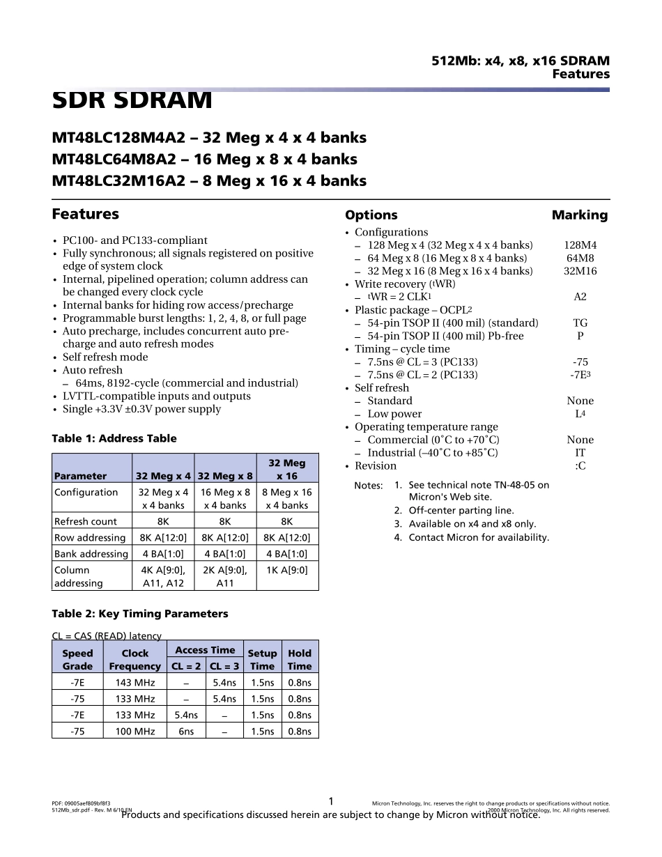
SDR SDRAMMT48LC128M4A2 – 32 Meg x 4 x 4 banksMT48LC64M8A2 – 16 Meg x 8 x 4 banksMT48LC32M16A2 – 8 Meg x 16 x 4 banksFeatures• PC100- and PC133-compliant• Fully synchronous; all signals registered on positiveedge of system clock• Internal, pipelined operation; column address canbe changed every clock cycle• Internal banks for hiding row access/precharge• Programmable burst lengths: 1, 2, 4, 8, or full page• Auto precharge, includes concurrent auto pre-charge and auto refresh modes• Self refresh mode• Auto refresh–64ms, 8192-cycle (commercial and industrial)• LVTTL-compatible inputs and outputs• Single +3.3V ±0.3V power supplyTable 1: Address TableParameter32 Meg x 4 32 Meg x 832 Megx 16Configuration32 Meg x 4x 4 banks16 Meg x 8x 4 banks8 Meg x 16x 4 banksRefresh count8K8K8KRow addressing8K A[12:0]8K A[12:0]8K A[12:0]Bank addressing4 BA[1:0]4 BA[1:0]4 BA[1:0]Columnaddressing4K A[9:0],A11, A122K A[9:0],A111K A[9:0]Table 2: Key Timing ParametersCL = CAS (READ) latencySpeedGradeClockFrequencyAccess TimeSetupTimeHoldTimeCL = 2CL = 3-7E143 MHz–5.4ns1.5ns0.8ns-75133 MHz–5.4ns1.5ns0.8ns-7E133 MHz5.4ns–1.5ns0.8ns-75100 MHz6ns–1.5ns0.8nsOptionsMarking• Configurations –128 Meg x 4 (32 Meg x 4 x 4 banks)128M4–64 Meg x 8 (16 Meg x 8 x 4 banks)64M8–32 Meg x 16 (8 Meg x 16 x 4 banks)32M16• Write recovery (tWR) –tWR = 2 CLK1A2• Plastic package – OCPL2 –54-pin TSOP II (400 mil) (standard)TG–54-pin TSOP II (400 mil) Pb-freeP• Timing – cycle time –7.5ns @ CL = 3 (PC133)-75–7.5ns @ CL = 2 (PC133)-7E3• Self refresh –StandardNone–Low powerL4• Operating temperature range –Commercial (0˚C to +70˚C)None–Industrial (–40˚C to +85˚C)IT• Revision:CNotes:1. See technical note TN-48-05 onMicron's Web site.2. Off-c...