1.利用双输入端的nand 门,用Verilog 编写自己的双输入端的与门、或门和非门,把它们分别命名为 my_or,my_and 和 my_not,并通过激励模块验证这些门的功能。 
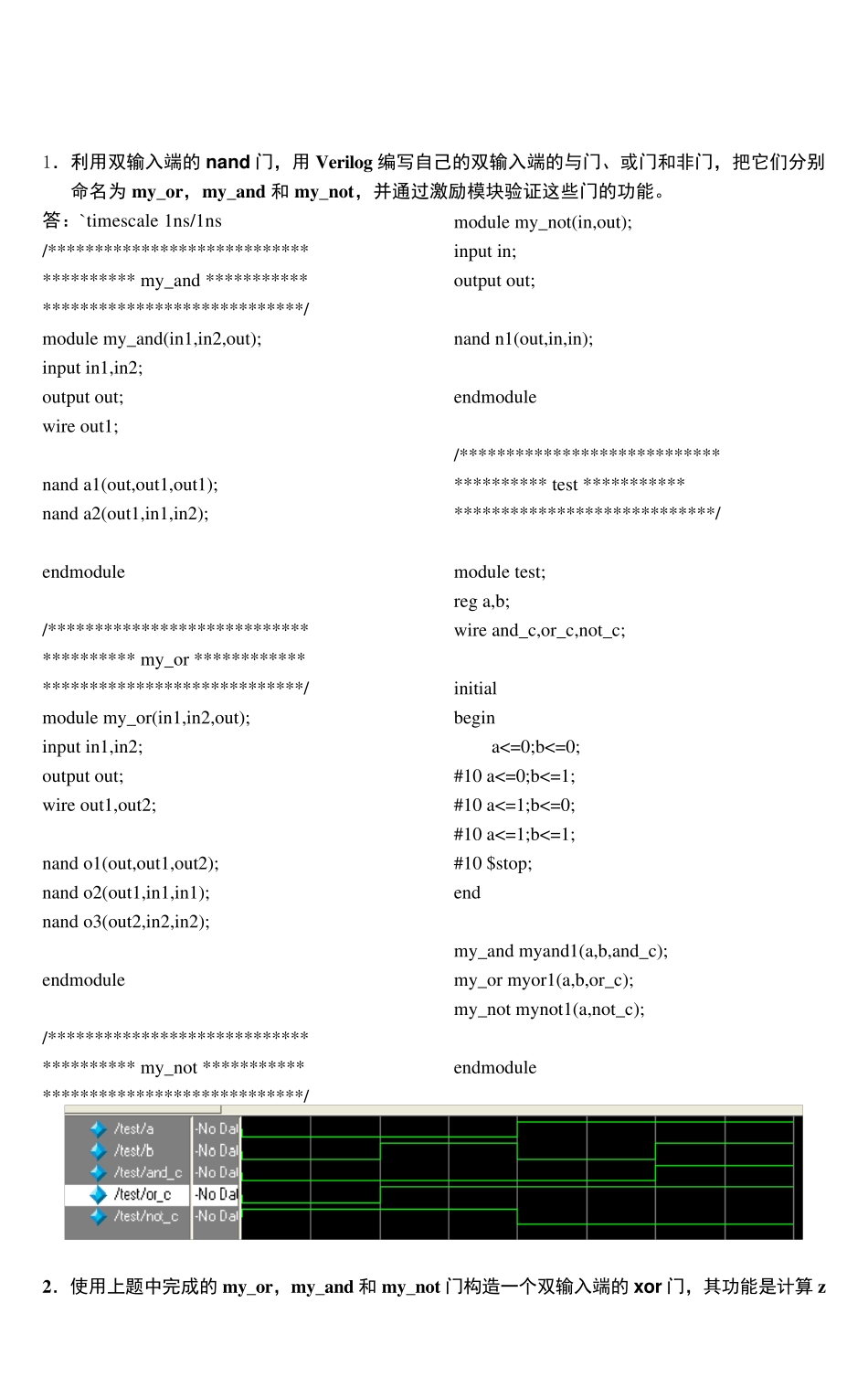
答:`timescale 1ns/1ns /**************************** ********** my_and *********** ****************************/ module my_and(in1,in2,out); input in1,in2; output out; wire out1; nand a1(out,out1,out1); nand a2(out1,in1,in2); endmodule /**************************** ********** my_or ************ ****************************/ module my_or(in1,in2,out); input in1,in2; output out; wire out1,out2; nand o1(out,out1,out2); nand o2(out1,in1,in1); nand o3(out2,in2,in2); endmodule /**************************** ********** my_not *********** ****************************/ module my_not(in,out); input in; output out; nand n1(out,in,in); endmodule /**************************** ********** test *********** ****************************/ module test; reg a,b; wire and_c,or_c,not_c; initial begin a<=0;b<=0; #10 a<=0;b<=1; #10 a<=1;b<=0; #10 a<=1;b<=1; #10 $stop; end my_and myand1(a,b,and_c); my_or myor1(a,b,or_c); my_not mynot1(a,not_c); endmodule 2.使用上题中完成的my_or,my_and 和 my_not 门构造一个双输入端的x or 门,其功能是计算 z 第5章 门 级 建 模 4 1 = x’y + x y’,其中x 和y 为输入,z 为输出;编写激励模块对x 和y 的四种输入组合进行测试仿真。 答:在上题代码的基础上,添加如下代码:(注意,xor 在仿真器中已自备,这里用 my_xor) /**************************** ********* my_xor ********** ********* z=x'y+xy' ********* ****************************/ module my_xor(in1,in2,out); input in1,in2; output out; wire not_in1,not_in2,out_a1,out_a2; my_not mynot1(in1,not_in1); my_not mynot2(in2,not_in2); my_and myand1(in1,not_in2,out_a1); my_and myand2(in2,not_in1,out_a2); my_or myor1(out_a1,out_a2,out); endmodule module test52; reg x,y; wire z; initial begin x<=0;y<=0; #10 x<=0;y<=1; #10 x<=1;y<=0;...