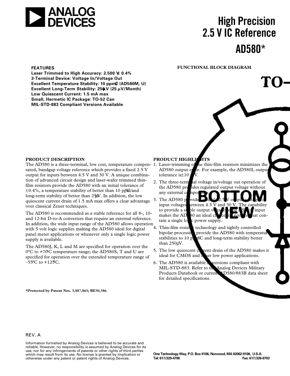
FUNCTIONAL BLOCK DIAGRAMREV. AInformation furnished by Analog Devices is believed to be accurate andreliable. However, no responsibility is assumed by Analog Devices for itsuse, nor for any infringements of patents or other rights of third partieswhich may result from its use. No license is granted by implication orotherwise under any patent or patent rights of Analog Devices.aHigh Precision2.5 V IC ReferenceAD580*One Technology Way, P.O. Box 9106, Norwood, MA 02062-9106, U.S.A.Tel: 617/329-4700Fax: 617/326-8703FEATURESLaser Trimmed to High Accuracy: 2.500 V ؎ 0.4%3-Terminal Device: Voltage In/Voltage OutExcellent Temperature Stability: 10 ppm/؇C (AD580M, U)Excellent Long-Term Stability: 250 V (25 V/Month)Low Quiescent Current: 1.5 mA maxSmall, Hermetic IC Package: TO-52 CanMIL-STD-883 Compliant Versions AvailablePRODUCT DESCRIPTIONThe AD580 is a three-terminal, low cost, temperature compen-sated, bandgap voltage reference which provides a fixed 2.5 Voutput for inputs between 4.5 V and 30 V. A unique combina-tion of advanced circuit design and laser-wafer trimmed thin-film resistors provide the AD580 with an initial tolerance of±0.4%, a temperature stability of better than 10 ppm/°C andlong-term stability of better than 250 µV. In addition, the lowquiescent current drain of 1.5 mA max offers a clear advantageover classical Zener techniques.The AD580 is recommended as a stable reference for all 8-, 10-and 12-bit D-to-A converters that require an external reference.In addition, the wide input range of the AD580 allows operationwith 5 volt logic supplies making the AD580 ideal for digitalpanel meter applications or whenever only a single logic powersupply is available.The AD580J, K, L and M are specified for operatio...