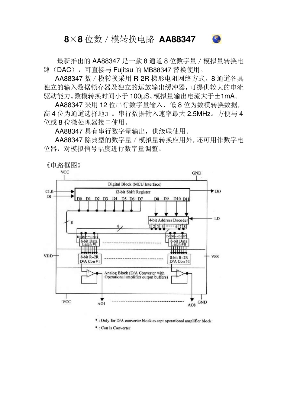
8×8 位数/模转换电路 A A 88347 最新推出的AA88347 是一款8 通道8 位数字量/模拟量转换电路(DAC),可直接与Fujitsu 的MB88347 替换使用
AA88347 数/模转换采用R-2R 梯形电阻网络方式
8 通道各具独立的输入数据锁存器及独立的运放输出缓冲器,可提供较大的电流驱动能力
数模转换时间小于100µS
模拟量输出电流大于±1mA
AA88347 采用12 位串行数字量输入,低 8 位为数模转换数据,高 4 位为通道选择地址
串行数据输入速率最大2
方便与4位或 8 位微处理器接口使用
AA88347 具有串行数字量输出,供级联使用
AA88347 除典型的数字量/模拟量转换应用外,还可用作数字电位器,对模拟信号幅度进行数字量调整
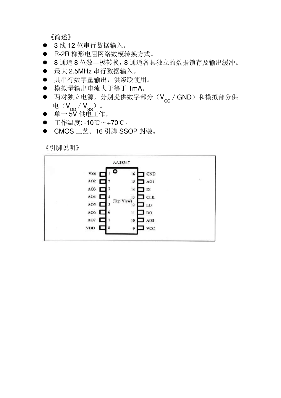
《电路框图》 《简述》 3 线12 位串行数据输入
R-2R 梯形电阻网络数模转换方式
8 通道8 位数—模转换,8 通道各具独立的数据锁存及输出缓冲
5MHz串行数据输入
具串行数字量输出,供级联使用
模拟量输出电流大于等于1mA
两对独立电源,分别提供数字部分(VCC/GND)和模拟部分供电(VDD/VSS)
单一5V 供电工作
工作温度: -10℃~+70℃
CMOS 工艺
16 引脚 SSOP 封装
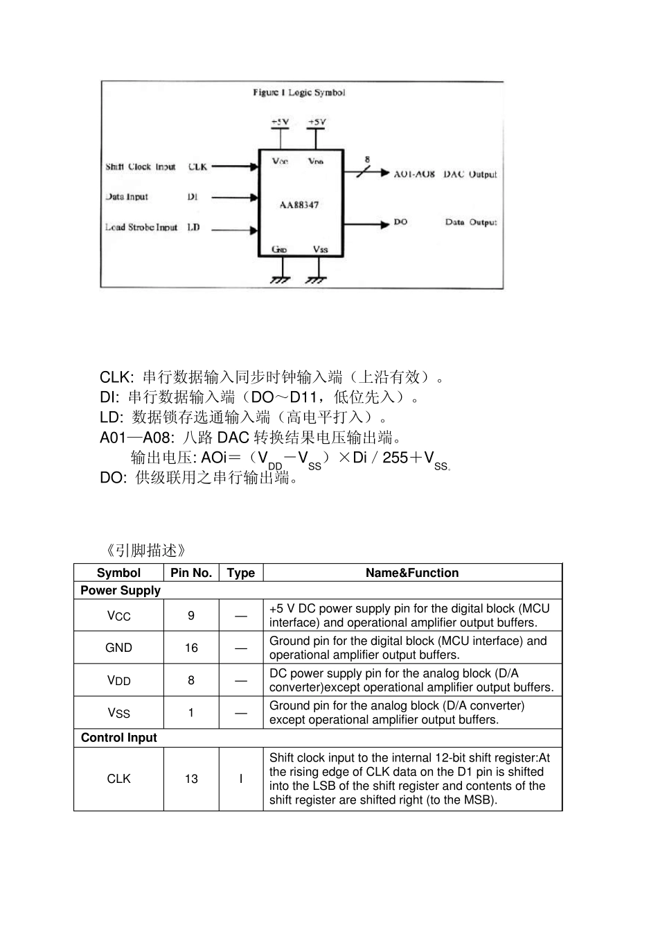
《引脚说明》 CLK: 串行数据输入同步时钟输入端(上沿有效)
DI: 串行数据输入端(DO~D11,低位先入)
LD: 数据锁存选通输入端(高电平打入)
A01—A08: 八路DAC 转换结果电压输出端
输出电压: AOi=(VDD-VSS)×Di/255+VSS
DO: 供级联用之串行输出端
《引脚描述》 Symbol Pin No
Type Name&Function Power Supply V